
Nidek Co., Ltd.
- Home
- Companies
- Nidek Co., Ltd.
- Products
- Nidek - Model FT-17 - Flatness Tester
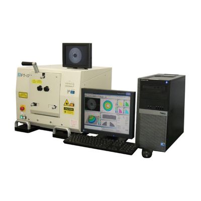
Nidek - Model FT-17 - Flatness Tester
FromNidek Co., Ltd.
The measured data can be quickly acquired by full surface analysis with laser light. The measurement result can be displayed as measured values, contour map, bird`s-eye view, cross-section view, etc. Original phase shift method is applicable to multiple interference fringes System control with exclusive analyzer running on the Windows platform provides easy operation. Transparent samples can not only be analyzed but also be measured with minimized interference of rear surface. The measurement result once obtained from sample data can be re-calculated to reflect changes in perimeter exclusion range, etc. Special calibration is unnecessary, pre-operation check with customer`s referential samples is recommended.
Most popular related searches
- Various software for each measurement of wafers, disks, square samples, user-defined shaped samples can be selectably used.
- Various Vacuum chucks for wafers enable High-precision GBIR (TTV) measurement
- Stepper simulation and Stress analysis software to meet the demands of wafers industry users
- Software for user-defined area enables partial measurement.
- Various types of cradles are available for each usage.
- Samples up to outer diameter φ130 mm are measurable. (Up to φ100 mm for flatness measurement)
- Applicable to wafers (silicon, compound, oxide or glass), metallic fragments, disks (aluminum or glass), or user-defined shaped parts, etc.
- Applicable to mirrored/non-mirrored surface, transparent samples, perforated samples, or atypical samples
- Various samples are digitally measurable by analyzing interference fringe pattern obtained by laser oblique incidence interferometer through the phase shift method.